Impress employers and recruiters.
Choose from hundreds of resume examples.

Impress employers and recruiters.
Choose from hundreds of resume examples.
Tailor your resume to this DFX Lead Engineeer role.
Rezi rewrites your resume against Ericsson's job description. Free.
Tailor your resume to this DFX Lead Engineeer role.
Rezi rewrites your resume against Ericsson's job description. Free.
Don't guess if your resume is good enough.
See how it scores against the DFX Lead Engineeer posting at Ericsson — free, in seconds.
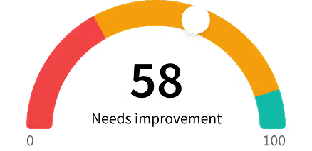
Don't guess if your resume is good enough.
See how it scores against the DFX Lead Engineeer posting at Ericsson — free, in seconds.
About the Role
As Senior DFX Lead, you are the technical owner of DFX and RAS for one or more ASIC programs. You set the DFX architecture and test strategy, drive IP and SoC-level integration with design and physical-design teams, own pattern delivery to test engineering, lead the design side of silicon bring-up and yield learning, and carry the same hooks into in-field test, monitoring, and repair. You design for the whole lifecycle - manufacturing test, SLM and in-field RAS - from day one, and what you architect is reused across programs and product generations.
Responsibilities
- Own DFX and SLM architecture for one or more ASIC programs, including the DFT plan, test strategy, and RAS requirements. Sign off DFX and SLM scope as a precondition for tape-out.
- Architect and drive the full DFX/SLM stack: scan and compression, ATPG, memory and logic BIST (with memory repair), JTAG/IJTAG and boundary scan (IEEE 1149.1, 1149.6, 1687), in-field test, and test access for custom, analog, and high-speed IP.
- Integrate DFX into RTL at IP and SoC level, own DFX timing constraints (SDC), and partner with physical design on implementation and timing sign-off.
- Own DFX/SLM verification: define and execute RTL and gate-level verification of the DFT, debug, and lifecycle-monitoring infrastructure across production-test and in-field use cases, including DFT rule checks and equivalence checking.
- Deliver test content to test engineering and silicon partners: pattern generation, fault simulation, coverage closure, and test-time optimization. Review test quality against DPPM targets with ASIC vendors.
- Define on-die debug and observability and lead the design side of bring-up, yield learning and failure analysis, closing the loop into the next tape-out.
- Shape the SLM architecture with the SLM team and enable the runtime applications built on it with systems, firmware and software teams.
- Advance the methodology: work with EDA vendors and CAD to define next-generation DFT flows and automate the DFX execution pipeline.
- Lead and grow the team: mentor DFX engineers, review their work, and represent DFX to architects, program management, and external partners.
Requirements
- 12+ years in SoC, IP, or ASIC design with an emphasis on DFX (DFT, DFD, DFM), including several years leading DFX on a complex SoC through tape-out on advanced process nodes.
- Expert, hands-on command of the DFX stack - scan and compression, ATPG, JTAG/IJTAG, boundary scan, memory and logic BIST - and the trade-offs between test quality, test time and area, and their impact on implementation.
- Hands-on experience with a production DFT flow.
- Proven ownership of SoC-level DFT planning, architecture and execution, and of DFX verification (memory BIST, JTAG, boundary scan, in-field tests, custom IP test interfaces).
- Post-silicon experience: bring-up, yield learning, test-time reduction, and pattern delivery, working closely with test and product engineering.
- Working knowledge of RTL (Verilog/SystemVerilog), synthesis, STA and clock/reset design, and of physical-design and timing-closure flows so DFT integrates cleanly.
- Ability to lead through influence: set direction, review others’ work, and be the DFX voice to architects, program management, and external partners, with clear written and spoken communication across sites and time zones.
Skills
- DFX
- DFT
- DFD
- DFM
- SLM
- RAS
- Scan and compression
- ATPG
- Memory and logic BIST
- JTAG/IJTAG
- Boundary scan
- In-field test
- Test access for custom, analog, and high-speed IP
- RTL integration
- Timing constraints (SDC)
- Physical design
- Timing sign-off
- DFX verification
- Pattern generation
- Fault simulation
- Coverage closure
- Test-time optimization
- On-die debug
- Observability
- Bring-up
- Yield learning
- Failure analysis
- Runtime applications
- Methodology advancement
- EDA vendor collaboration
- CAD collaboration
- Team leadership
- Mentoring
- Work-life balance
- Verilog/SystemVerilog
- Synthesis
- STA
- Clock/reset design
- On-die sensors and monitors
- Fault logging
- Telemetry
- In-field diagnostics
- Firmware/SDK
- Chiplet design
- 2.5D/3D design
- System-level test (SLT)
- Functional ATE pattern enablement
- Functional-safety
- High-reliability products
- ASIC vendor partnership
- Wireless infrastructure ASICs
- Networking ASICs
- Compute ASICs
Location
- Austin, Texas
Work Type
- Hybrid
- On-Site
Experience Level
- Senior
- 12+ years
Education Level
- BSEE
- MSEE preferred
Salary/Compensations
- The salary range for this position is dependent on various factors including, but not limited to, location, and the candidate’s combination of job-related knowledge, qualifications, skills, education, training, and experience.
- Opportunity for an annual bonus based on business and individual performance.
Benefits
- Choice of three medical plan options
- Dental plan option
- Company credits towards medical and dental premiums
- Ericsson US 401(k) Plan with automatic 3% company contribution
- Ericsson 401(k) match up to 4%
- Company credits for basic life insurance and basic accidental death and dismemberment coverage
- Company credits for short-term and long-term disability coverage
- Optional participation in Ericsson’s Stock Purchase Plan
- Minimum of 15 days of accrued vacation
- Up to 3 personal days per year
- 11 annual holidays
- 8 hours of volunteer time
- 80 hours of sick time annually
- Up to 16 weeks of paid maternity leave
- 6 weeks of parental or adoption leave at 100% of pay
- Financial wellness programs
- Educational assistance
- Matching gifts
- Recognition programs
About the Company
- Ericsson's Radio and Baseband products run on ASICs we design ourselves, at the most advanced process nodes, and every silicon must be testable, debuggable, and observable throughout its life in the field.
- The Austin DFX & SLM team owns DFX, Silicon Lifecycle Management (SLM) and Reliability, Availability and Serviceability (RAS) for every ASIC across Ericsson's product line, from requirements and architecture through IP and SoC integration to silicon bring-up and in-field operation.
- Your work ends up in networks that connect billions of people - and you see your designs through from requirements to working silicon in the lab, in production test, and in the field for years afterward.
- You will own DFX, RAS, and SLM architecture that is reused across every ASIC in the product line, working beside engineers who built this capability from the ground up, in a global team with a speak-up culture and a real commitment to work-life balance.
Equal Opportunity
- Diversity and inclusion are core to our values, and collaboration across different experiences drives the innovation essential to our growth. Ericsson is proud to be an Equal Opportunity Employer.
- Ericsson uses a merit-based hiring approach that values people with different experiences, perspectives and skillsets. We truly believe this approach drives innovation, which is essential for our future growth. We encourage people from all backgrounds to apply and realize their full potential as part of our Ericsson team.
- Ericsson is proud to be an Equal Opportunity employer, learn more.