Impress employers and recruiters.
Choose from hundreds of resume examples.
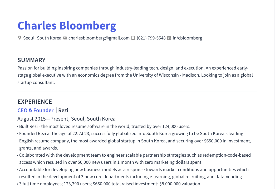
Impress employers and recruiters.
Choose from hundreds of resume examples.
Tailor your resume to this Engineer, Analysis Engineering role.
Rezi rewrites your resume against Samsung Electronics's job description. Free.
Tailor your resume to this Engineer, Analysis Engineering role.
Rezi rewrites your resume against Samsung Electronics's job description. Free.
Don't guess if your resume is good enough.
See how it scores against the Engineer, Analysis Engineering posting at Samsung Electronics — free, in seconds.
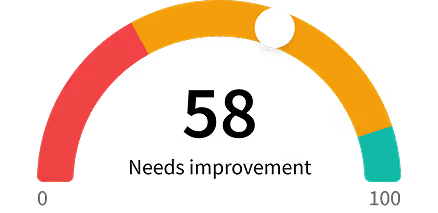
Don't guess if your resume is good enough.
See how it scores against the Engineer, Analysis Engineering posting at Samsung Electronics — free, in seconds.
About the Role
Samsung Austin Semiconductor is seeking an Engineer, Analysis Engineering to conduct physical failure analysis on various types of requests, identify root causes of failures, and support manufacturing and engineering teams.
Responsibilities
- Conduct physical failure analysis (pFA) on low yield lots, baseline material, qualifications, and customer returned samples.
- Identify failure causes by selecting appropriate samples and optimal analysis techniques.
- Support manufacturing and engineering teams with pFA results for new process introduction (NPI) and product transfer activities.
- Represent the Analysis Engineering department in foundry customer meetings by providing timely analysis results.
- Analyze electrical and imaging results to find root causes and publish findings.
- Recommend analysis approaches based on customer failure mode data and internal electrical isolation results.
- Generate and compile high-quality FA reports for internal and external customers.
- Develop methods to improve team analysis capability and reduce job turnaround time.
Requirements
- Master’s degree in Materials Science, Materials Engineering or a related field.
- Completion of an undergraduate-level course, research project, or internship involving: Monitoring and debugging test failures; Defect monitoring, characterization, and root cause analysis; Semiconductor manufacturing/fabrication process; Material Characterization Tools; Lab/fab operation; Semiconductor electrical performance; Design of experiment/testing; Semiconductor chemistry; Process/yield improvement; Thin Film Science; Nanotechnology; and Quality monitoring.
Skills
- Physical failure analysis
- Sample selection
- Analysis techniques
- Electrical analysis
- Imaging analysis
- Root cause analysis
- FA report generation
- Method development
Location
- Austin, TX
Work Type
- Full-time
- On-site
Education Level
- Master's degree
Salary/Compensations
- $110,598 to $130,598
Benefits
- Medical, dental, and vision insurance
- Life insurance
- 401(k) matching with immediate vesting
- Onsite café(s)
- Onsite workout facilities
- Paid maternity and paternity leave
- Paid time off (PTO)
- 2 personal holidays
- 10 regular holidays
- Wellness incentives
- MBO bonuses
About the Company
- Samsung is a world leader in advanced semiconductor technology.
- At Samsung Austin Semiconductor, we are Innovating Today to Power the Devices of Tomorrow.
Equal Opportunity
- Samsung Electronics America, Inc. and its subsidiaries are committed to Equal Employment Opportunity for all individuals regardless of race, color, religion, gender, age, national origin, marital status, sexual orientation, gender identity, status as a protected veteran, genetic information, status as a qualified individual with a disability, or any other characteristic protected by law.