Impress employers and recruiters.
Choose from hundreds of resume examples.

Impress employers and recruiters.
Choose from hundreds of resume examples.
Tailor your resume to this PCB Design Engineer role.
Rezi rewrites your resume against Wellington Steele & Associates's job description. Free.
Tailor your resume to this PCB Design Engineer role.
Rezi rewrites your resume against Wellington Steele & Associates's job description. Free.
Don't guess if your resume is good enough.
See how it scores against the PCB Design Engineer posting at Wellington Steele & Associates — free, in seconds.
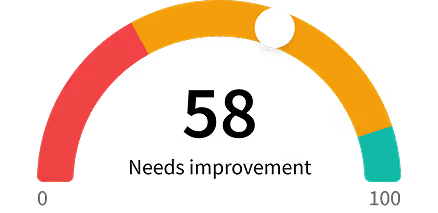
Don't guess if your resume is good enough.
See how it scores against the PCB Design Engineer posting at Wellington Steele & Associates — free, in seconds.
About the Role
We are seeking a Senior PCB Design Engineer to join our product development team. This role involves transforming ideas into manufacturable products by collaborating with cross-functional engineering teams and addressing complex layout challenges to optimize designs for performance and manufacturability.
Responsibilities
- Design PCB layouts for digital, mixed-signal, power, RF, and wireless products from concept through production.
- Collaborate with hardware, firmware, RF, and mechanical engineers to meet design and performance requirements.
- Create and maintain schematics, symbols, footprints, and component libraries.
- Define PCB stack-ups and support controlled impedance, differential pair routing, DDR signaling, and signal integrity requirements.
- Perform or support signal integrity analysis of critical interfaces.
- Partner with PCB fabricators and assembly suppliers during prototype and production builds.
- Review designs for manufacturability, testability, reliability, and cost optimization.
- Support EMC and regulatory compliance through best-practice PCB design techniques.
- Resolve technical issues related to PCB fabrication and assembly.
- Contribute to PCB design standards, libraries, and engineering process improvements.
- Collaborate with global engineering teams to share best practices and support new product development initiatives.
Requirements
- Bachelor's degree in Electrical Engineering, Electrical Engineering Technology, or related field.
- 5+ years of PCB design experience, or equivalent combination of education and experience.
- Experience designing multi-layer PCBs for production environments.
- Strong understanding of schematic capture and PCB layout methodologies.
- Ability to manage multiple design activities with limited supervision.
- Strong organizational, communication, and problem-solving skills.
- Demonstrated ownership and accountability for project deliverables.
Skills
- High-speed digital interfaces
- RF technologies including Zigbee and LoRa
- Mixed-signal and power electronics
- Controlled impedance and differential pair routing
- Signal integrity analysis
- Multi-layer PCB design (2, 4, 6+ layers)
- EMC and regulatory compliance-focused design
- Siemens Xpedition
- Mentor Graphics PADS
- DxDesigner
- Altium Designer
- Matched-length routing
- DDR designs
- PCB manufacturing
- Assembly
- DFM
- DFA
- HyperLynx
- PCB materials
- Fabrication processes
- Impedance control techniques
- AutoCAD
- PTC Creo
- IPC CID or CID+ certification
Location
- Fairport, NY
Work Type
- Full-time
Experience Level
- Senior
- 5+ years
Education Level
- Bachelor's degree