Impress employers and recruiters.
Choose from hundreds of resume examples.
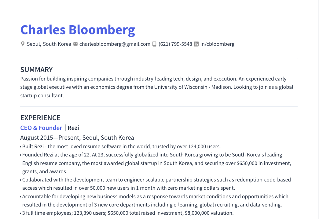
Impress employers and recruiters.
Choose from hundreds of resume examples.
Tailor your resume to this Physical Design Engineering Director role.
Rezi rewrites your resume against Astera Labs's job description. Free.
Tailor your resume to this Physical Design Engineering Director role.
Rezi rewrites your resume against Astera Labs's job description. Free.
Don't guess if your resume is good enough.
See how it scores against the Physical Design Engineering Director posting at Astera Labs — free, in seconds.
Don't guess if your resume is good enough.
See how it scores against the Physical Design Engineering Director posting at Astera Labs — free, in seconds.
About the Role
Astera Labs is seeking a Physical Design Engineering Director to lead a team of physical design engineers at our Toronto site, driving the implementation of connectivity ASICs within our Signal Connectivity Group. This group is responsible for products that enable high-speed serial connectivity including PCIe retimers, Ethernet retimers, and signal conditioning solutions deployed across the world's largest AI clusters and hyperscale data centers. You will combine hands-on technical leadership with people management, owning physical design execution from RTL to GDSII while building and mentoring a high-performing team. You will drive floorplanning, place-and-route, timing closure, and sign-off for complex designs requiring deep understanding of high-speed physical layer interfaces and SerDes integration at TSMC advanced nodes.
Responsibilities
- Build, lead, and mentor a physical design team, owning Physical Design execution and team development for Signal Connectivity Group products.
- Drive block and top-level physical design implementation from floorplan through tapeout for retimer and signal conditioning ASICs.
- Collaborate with RTL, DFT, STA, EMIR, and verification teams to drive design convergence from synthesis through sign-off.
- Work with IP vendors for both RTL and hard-macro integration, ensuring placement constraints and routing guidelines are met.
- Drive team execution, hiring, career development, and sprint planning for the Toronto PD team.
- Establish physical design best practices, flow improvements, and quality checks to scale execution across multiple concurrent programs.
- Coordinate with global PD teams (San Jose, Irvine, Bangalore) to ensure consistent methodology and design quality.
Requirements
- Bachelor's degree in Electrical Engineering, Computer Engineering, or a related field; Master's preferred.
- 15+ years of experience in physical design implementation of complex SoCs at advanced nodes (7nm and below).
- 5+ years of experience leading teams or projects with demonstrated ability to mentor and develop engineers.
- Hands-on expertise across the physical design flow: synthesis, place-and-route, CTS, extraction, timing closure, EM-IR, DRC/LVS, and equivalence checking.
- Proficiency with Cadence Innovus and/or Synopsys Fusion Compiler/ICC2 and supporting toolchains.
- Strong scripting ability in Tcl, Python, and/or Perl.
- Professional attitude with the ability to prioritize a dynamic list of tasks, plan and prepare for customer meetings in advance, and work with minimal guidance.
- Entrepreneurial, open-minded behavior and can-do attitude. Think and act fast with the customer in mind!
Skills
- Physical design implementation
- SoC design
- Advanced nodes (7nm and below)
- Team leadership
- Mentoring engineers
- Physical design flow
- Synthesis
- Place-and-route
- CTS
- Extraction
- Timing closure
- EM-IR
- DRC/LVS
- Equivalence checking
- Cadence Innovus
- Synopsys Fusion Compiler/ICC2
- Tcl scripting
- Python scripting
- Perl scripting
- High-speed SerDes physical layer
- Equalization
- CDR
- Signal integrity
- Physical layer timing challenges
- EDA automation
Location
- Toronto
Work Type
- On-site
Experience Level
- 15+ years of experience in physical design implementation of complex SoCs at advanced nodes (7nm and below)
- 5+ years of experience leading teams or projects
Education Level
- Bachelor's degree in Electrical Engineering, Computer Engineering, or a related field
- Master's preferred
Salary/Compensations
- CAD 200,000 to CAD 250,000
Benefits
- Discretionary bonus
- Incentives
About the Company
- Astera Labs (NASDAQ: ALAB) provides rack-scale AI infrastructure through purpose-built connectivity solutions.
- By collaborating with hyperscalers and ecosystem partners, Astera Labs enables organizations to unlock the full potential of modern AI.
- Astera Labs’ Intelligent Connectivity Platform integrates CXL®, Ethernet, NVLink, PCIe®, and UALink™ semiconductor-based technologies with the company’s COSMOS software suite to unify diverse components into cohesive, flexible systems that deliver end-to-end scale-up, and scale-out connectivity.
- The company’s custom connectivity solutions business complements its standards-based portfolio, enabling customers to deploy tailored architectures to meet their unique infrastructure requirements.
Equal Opportunity
- We know that creativity and innovation happen more often when teams include diverse ideas, backgrounds, and experiences, and we actively encourage everyone with relevant experience to apply, including people of color, LGBTQ+ and non-binary people, veterans, parents, and individuals with disabilities.