Impress employers and recruiters.
Choose from hundreds of resume examples.
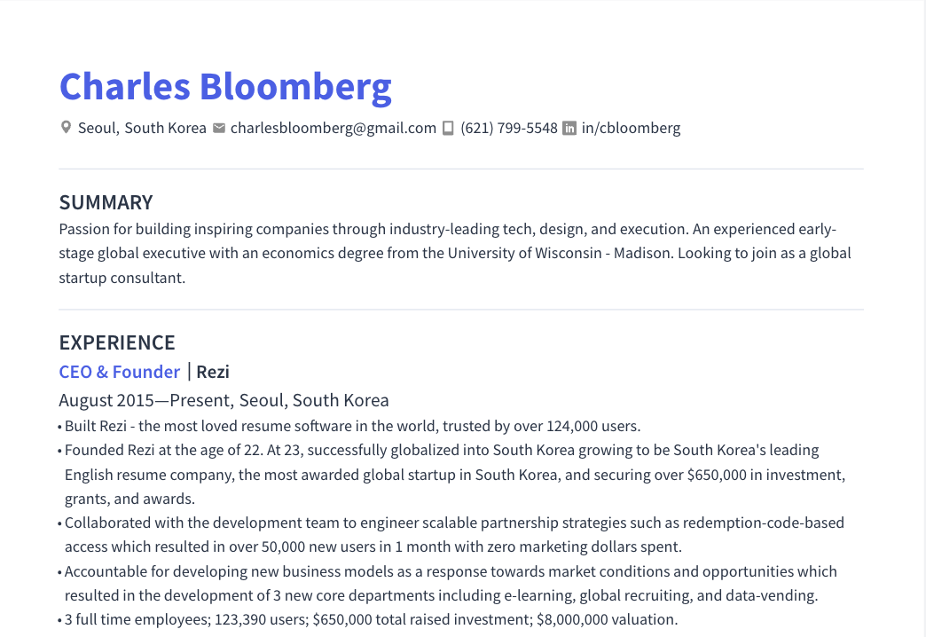
Impress employers and recruiters.
Choose from hundreds of resume examples.
Tailor your resume to this ASIC Package Engineer role.
Rezi rewrites your resume against Meta's job description. Free.
Tailor your resume to this ASIC Package Engineer role.
Rezi rewrites your resume against Meta's job description. Free.
Don't guess if your resume is good enough.
See how it scores against the ASIC Package Engineer posting at Meta — free, in seconds.
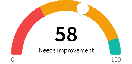
Don't guess if your resume is good enough.
See how it scores against the ASIC Package Engineer posting at Meta — free, in seconds.
About the Role
Meta is seeking an experienced ASIC Package Engineer to lead the technology development and qualification of the package-to-board attach process for custom AI/ML and networking silicon. This role is crucial for ensuring the reliable interface between advanced packages and motherboards in Meta's global data centers.
Responsibilities
- Own package-to-board interaction technology development for Meta's large-body advanced packages, focusing on the behavior of the package, substrate, and PCB during assembly and in the field.
- Characterize and mitigate package warpage and coplanarity across the reflow window for large-body and lidless packages.
- Drive board-level reliability (BLR) strategy for ASIC packages in partnership with quality teams, covering thermal cycling, drop/shock, bend, and vibration.
- Define and execute mechanical and electrical test vehicle (MTV/ETV) strategies to de-risk package-board interaction before A0 silicon availability, including solder-joint evaluation.
- Represent package-board interaction and board-assembly constraints in silicon/package/PCB/system co-design and product design reviews.
- Collaborate with package design and module design teams to ensure design for manufacturability (DFM) considerations are integrated into package and board development.
- Develop and implement package-board interaction process specifications, design rules, and manufacturing guidelines for new package technologies.
- Evaluate and qualify new package-board interaction equipment, materials, and processes to support technology roadmap requirements.
- Partner with PQE, SQE, and ARD teams to establish quality standards, qualification criteria, and reliability requirements for package-board interaction processes.
- Establish statistical process control (SPC) methodologies and yield improvement initiatives for package-board interaction assembly operations.
- Own package-board interaction content in FMEAs, control plans, and key-characteristic definitions; support ODM line qualification and control-run gates with PQE.
- Create, conduct, and analyze Designs of Experiments (DOE) for package-board interaction development and sustaining activities.
- Drive supplier engagement and qualification for package-board interaction-related materials and equipment.
Requirements
- Bachelor's degree in Computer Science, Computer Engineering, relevant technical field, or equivalent practical experience.
- Master's degree in Materials Science, Mechanical Engineering, Electrical Engineering, or a related field, or equivalent practical experience.
- 8+ years of experience in semiconductor packaging with direct ownership of package-to-board assembly and reliability; package-board interaction process engineering or electronics manufacturing background.
- Experience with package board technology processes including solder paste printing, pick-and-place, reflow soldering, and inspection methods.
- Experience working with package assembly and ODM suppliers and driving process qualification and yield improvement programs.
- Experience with failure analysis techniques for solder joint reliability and package-board interaction-related defects.
- Experience collaborating with quality engineering teams (PQE/SQE) to establish process controls and qualification requirements.
- Experience with statistical process control, process capability analysis, and Design of Experiments.
- Willingness to travel internationally, typically once per quarter.
Skills
- Package-to-board interaction technology development
- Package warpage and coplanarity characterization and mitigation
- Board-level reliability (BLR) strategy
- Mechanical and electrical test vehicle (MTV/ETV) strategies
- Solder-joint evaluation
- Design for manufacturability (DFM)
- Process specifications, design rules, and manufacturing guidelines
- Equipment, materials, and process qualification
- Quality standards, qualification criteria, and reliability requirements
- Statistical process control (SPC)
- Yield improvement initiatives
- Failure Mode and Effects Analysis (FMEA)
- Control plans
- Key-characteristic definitions
- Design of Experiments (DOE)
- Supplier engagement and qualification
- Reflow temperature profiling
- Solder alloy and paste material selection
- Low-temperature solder processes
- AI/HPC or networking hardware at data-center scale
- High-temperature warpage characterization
- Thermo-mechanical or finite element modeling (FEM)
- SPI, AOI, and X-ray inspection systems
- Large-body FCBGA, flip-chip, and 2.5D/3D advanced packages
- ODM, CM/EMS, OSAT, and substrate supplier engagement and audit
Location
- Worldwide
Work Type
- Full-time
Experience Level
- 8+ years of experience in semiconductor packaging
Education Level
- Bachelor's degree in Computer Science, Computer Engineering, relevant technical field, or equivalent practical experience
- Master's degree in Materials Science, Mechanical Engineering, Electrical Engineering, or a related field, or equivalent practical experience
- Master's degree or PhD in Materials Science, Mechanical Engineering, or a related discipline
Salary/Compensations
- $178,000/year to $250,000/year
Benefits
- bonus
- equity
- benefits
About the Company
- Meta Infrastructure team designs, builds, brings up, tests, and integrates custom and general-purpose silicon-based hardware systems that power Meta's platforms, deployed in data centers worldwide.
- Designs are published through the Open Compute Project Foundation.
- We are building a deep competency in packaging technology to support the rapid development of custom silicon and to develop scalable packaging solutions that are optimal for our next-generation AI/ML products and system-level performance.
- As die sizes grow past 3.3x reticle and packages move to lidless/lidded and asymmetric stackups, board technology development for next gen ASIC is very important to achieve desired yield due to challenges with package warpage, thermo-mechanical stresses, and solder-joint reliability.