Impress employers and recruiters.
Choose from hundreds of resume examples.
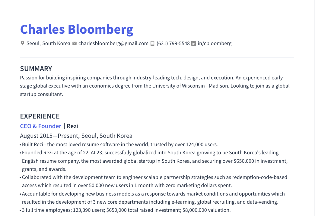
Impress employers and recruiters.
Choose from hundreds of resume examples.
Tailor your resume to this Photo Equipment Engineer role.
Rezi rewrites your resume against Samsung Electronics's job description. Free.
Tailor your resume to this Photo Equipment Engineer role.
Rezi rewrites your resume against Samsung Electronics's job description. Free.
Don't guess if your resume is good enough.
See how it scores against the Photo Equipment Engineer posting at Samsung Electronics — free, in seconds.
Don't guess if your resume is good enough.
See how it scores against the Photo Equipment Engineer posting at Samsung Electronics — free, in seconds.
About the Role
The Photolithography department focuses on delivering solutions by developing 24x7x365 teams of elite, fab-oriented, excursion-free, safety and quality minded members. As part of the Photo Equipment Engineering team, you will work together to support one another and our customers regardless of organizational boundaries. The Spinner Equipment Engineer will be actively transferring next generation technology including Spinner and auxiliary equipment installation, qualification and recipe transfer.
Responsibilities
- Performing Spinner and auxiliary equipment installation, including hardware and product qualification.
- Creating next generation technology node transfer including recipes, SOPs, BKMs.
- Attending and contributing in daily tactical meetings with vendors and internal teams about photolithography equipment; and attending weekly meetings with vendors and internal teams including strategic cross-functional meetings regarding equipment metrics and contribute to department and sites improvement plans.
- Coordinating Samsung internal, external and multiple vendor resources to provide optimum manufacturing support on assigned equipment.
- Investigating, troubleshooting and providing technical solutions to equipment related defect, quality and yield problems.
- Analyzing and reporting tool performance data, including availability, mean time to repair, mean time between failures, particle and defect trends, maintenance success, and similar metrics for assigned equipment.
- Providing weekend coverage as needed (~ 12 weeks a year). You will be responsible for multiple tools on the weekend larger than your normal scope and required to make tactical decisions based on your assessment of the daily operations environment in order to successfully achieve KPI.
Requirements
- 4 years of college in related field.
- 5+ years of semiconductor Photo or Cleans equipment ownership.
- In-depth experience on one or more of the following types of semiconductor equipment: SEMES, TEL, Screen.
- Understanding of semiconductor wafer processing fundamentals and photolithography.
- Familiarity with SPC, FMEA, FDC, yield analysis and other standard engineering and manufacturing practices.
- Ability to travel internationally as needed.
- Employment may be contingent on either the applicant verifying that the applicant falls under the “U.S. Person” definition (including U.S. citizens, U.S. lawful permanent residents, and those granted U.S. asylum or refugee status) or the employer timely obtaining any necessary export license under federal law.
- By submitting an application, you agree not to disclose to Samsung or induce or encourage Samsung to use any confidential or proprietary information (including trade secrets) belonging to a current or former employer or other entity.
Skills
- Spinner and auxiliary equipment installation
- Hardware and product qualification
- Next generation technology node transfer
- Recipes, SOPs, BKMs
- Vendor and internal team meetings
- Equipment metrics analysis
- Department and site improvement plans
- Manufacturing support
- Troubleshooting equipment related defect, quality and yield problems
- Tool performance data analysis
- Availability, mean time to repair, mean time between failures, particle and defect trends, maintenance success analysis
- Tactical decision making
- SEMES equipment
- TEL equipment
- Screen equipment
- Semiconductor wafer processing fundamentals
- Photolithography
- SPC
- FMEA
- FDC
- Yield analysis
Location
- Austin
Work Type
- Full-time
- On-site
Experience Level
- 5+ years of semiconductor Photo or Cleans equipment ownership
Education Level
- 4 years of college in related field
Salary/Compensations
- $106,000 - $145,000
Benefits
- Medical, dental, and vision insurance
- Life insurance
- 401(k) matching with immediate vesting
- Onsite café(s)
- Onsite workout facilities
- Paid maternity leave
- Paid paternity leave
- Paid time off (PTO)
- 2 personal holidays
- 10 regular holidays
- Wellness incentives
- MBO bonuses
About the Company
- Samsung is a world leader in advanced semiconductor technology, founded on the belief that the pursuit of excellence creates a better world.
- At Samsung Austin Semiconductor, we are Innovating Today to Power the Devices of Tomorrow.
- Samsung Austin Semiconductor will boost the production of semiconductor solutions that will power next-generation technologies in areas like 5G, artificial intelligence (AI) and high-performance computing (HPC).
- With greater manufacturing capacity, we will be able to better serve the needs of our customers and contribute to the stability of the global semiconductor supply chain.
Equal Opportunity
- Samsung Electronics America, Inc. and its subsidiaries are committed to Equal Employment Opportunity for all individuals regardless of race, color, religion, gender, age, national origin, marital status, sexual orientation, gender identity, status as a protected veteran, genetic information, status as a qualified individual with a disability, or any other characteristic protected by law.