Process Integrator Advanced Packaging & Co-Packaged Optics R&D
Applied Materials · Albany, NY, US
24 days agoImpress employers and recruiters.
Choose from hundreds of resume examples.
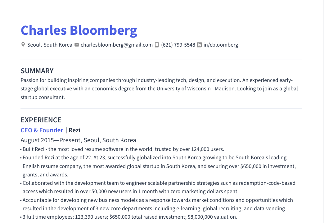
Impress employers and recruiters.
Choose from hundreds of resume examples.
Tailor your resume to this Process Integrator Advanced Packaging & Co-Packaged Optics R&D role.
Rezi rewrites your resume against Applied Materials's job description. Free.
Tailor your resume to this Process Integrator Advanced Packaging & Co-Packaged Optics R&D role.
Rezi rewrites your resume against Applied Materials's job description. Free.
Don't guess if your resume is good enough.
See how it scores against the Process Integrator Advanced Packaging & Co-Packaged Optics R&D posting at Applied Materials — free, in seconds.
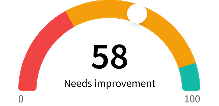
Don't guess if your resume is good enough.
See how it scores against the Process Integrator Advanced Packaging & Co-Packaged Optics R&D posting at Applied Materials — free, in seconds.
About the Role
We are seeking an experienced Process Integrator to lead development and integration of advanced semiconductor packaging modules in an R&D environment. This role will connect unit processes, materials, device requirements, metrology, reliability, and equipment capabilities into robust integrated flows. The successful candidate will work across Applied Materials business units, external partners, and customers to convert complex technical objectives into executable integration plans, learning cycles, and differentiated solutions. Experience in co-packaged optics (CPO), photonics packaging, or optical/electrical heterogeneous integration is strongly preferred.
Responsibilities
- Own end-to-end process integration for advanced packaging and heterogeneous integration programs, from initial concept and architecture through demonstration and technology transfer.
- Develop integrated process flows for photonic integrated circuits, electronic ICs, optical engines, interposers, substrates, and fiber interfaces, including module sequences, process windows, control plans, and learning-cycle strategies.
- Translate optical, electrical, thermal, mechanical, reliability, and manufacturability requirements into process-integration specifications and measurable success criteria for CPO modules.
- Lead cross-functional execution across photonics, device, packaging, bonding, lithography, deposition, etch, clean, CMP, plating, metrology, optical test, electrical test, failure analysis, modeling, and reliability teams.
- Drive integration of photonic and electronic die, including die-to-wafer or wafer-to-wafer bonding, fine-pitch interconnects, optical coupling and alignment, fiber attach interfaces, and advanced substrate or interposer integration.
- Design and execute structured experiments and DOEs to optimize optical loss, coupling efficiency, alignment tolerance, interconnect performance, thermal behavior, defectivity, yield, and reliability.
- Integrate laser, modulator, detector, waveguide, electronic IC, thermal-management, and package-level requirements into stable module and full-flow performance.
- Identify and resolve CPO integration risks such as contamination, bonding defects, overlay and alignment error, warpage, thermal-mechanical stress, optical-interface degradation, and process-induced device shifts.
- Create CPO technology roadmaps, integration reviews, risk assessments, schedules, and executive-ready reports; communicate clearly with engineers, senior leaders, customers, research partners, and suppliers.
- Identify invention opportunities, contribute to intellectual property, and establish disciplined R&D practices for CPO integration, data quality, documentation, and technical decision-making.
Requirements
- MS or PhD in Materials Science, Chemical Engineering, Electrical Engineering, Mechanical Engineering, Applied Physics, Photonics, or a related technical field.
- 5–10 years of experience in a semiconductor process integrator or process-integration role, with substantial experience in R&D or advanced technology development.
- Demonstrated experience building and executing integrated semiconductor or photonics process flows involving multiple process modules and cross-functional engineering teams.
- Strong understanding of CPO, silicon photonics, photonic integrated circuits, optical engines, or optical/electrical heterogeneous integration.
- Working knowledge of photonic and electronic die integration, optical coupling and alignment, fiber attach interfaces, fine-pitch interconnects, and advanced substrate or interposer integration.
- Understanding of optical loss, alignment tolerances, thermal management, thermal-mechanical interactions, packaging-induced stress, defect mechanisms, metrology, characterization, and reliability.
- Experience planning experiments, applying statistical analysis and DOE methods, interpreting optical, electrical, physical, and reliability datasets, and converting results into clear technical decisions.
- Proven ability to lead technically complex R&D projects with ambiguity, risk, and interdependencies while maintaining execution discipline.
- Self-directed, collaborative, and comfortable working in a fast-paced global R&D organization.
- Excellent written and verbal communication skills, including the ability to explain complex CPO integration issues to diverse technical and executive audiences.
Skills
- Co-packaged optics (CPO)
- Photonics packaging
- Optical/electrical heterogeneous integration
- Semiconductor process integration
- Advanced packaging
- Silicon photonics
- Photonic integrated circuits
- Optical engines
- Die-to-wafer bonding
- Wafer-to-wafer bonding
- Fine-pitch interconnects
- Optical coupling and alignment
- Fiber attach interfaces
- Advanced substrate integration
- Interposer integration
- DOE methods
- Statistical analysis
- Technical leadership
Location
- Albany, New York
- Santa Clara, CA
Work Type
- On-site
- Full time
Experience Level
- 5–10 years of experience in a semiconductor process integrator or process-integration role, with substantial experience in R&D or advanced technology development.
Education Level
- MS or PhD in Materials Science, Chemical Engineering, Electrical Engineering, Mechanical Engineering, Applied Physics, Photonics, or a related technical field.
Salary/Compensations
- $176,000.00 - $242,000.00
Benefits
- Supportive work culture that encourages learning, development, and career growth.
- Empowerment to push boundaries and drive innovative solutions.
- Opportunities for continuous learning in a supportive global company.
- Comprehensive benefits package.
- Potential eligibility for other forms of compensation such as bonus and stock awards.
- Relocation assistance.
About the Company
- Applied Materials is the global leader in materials science and engineering solutions.
- The equipment created and serviced is essential to advancing AI and accelerating the commercialization of next-generation semiconductor chips.
- The company's work advances the world's technology.
Equal Opportunity
- Applied Materials is an Equal Opportunity Employer. Qualified applicants will receive consideration for employment without regard to race, color, national origin, citizenship, ancestry, religion, creed, sex, sexual orientation, gender identity, age, disability, veteran or military status, or any other basis prohibited by law.
- Applied endeavors to make our careers site accessible to all users. If you would like to contact us regarding accessibility of our website or need assistance completing the application process, please contact us via e-mail at Accommodations_Program@amat.com, or by calling our HR Direct Help Line at 877-612-7547, option 1, and following the prompts to speak to an HR Advisor. This contact is for accommodation requests only and cannot be used to inquire about the status of applications.