Impress employers and recruiters.
Choose from hundreds of resume examples.
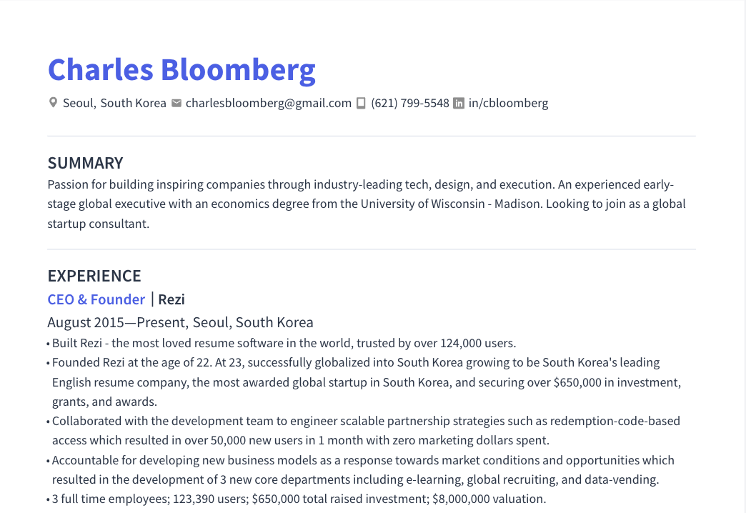
Impress employers and recruiters.
Choose from hundreds of resume examples.
Tailor your resume to this Physical Design Engineer- Staff to Sr. Staff role.
Rezi rewrites your resume against Qualcomm's job description. Free.
Tailor your resume to this Physical Design Engineer- Staff to Sr. Staff role.
Rezi rewrites your resume against Qualcomm's job description. Free.
Don't guess if your resume is good enough.
See how it scores against the Physical Design Engineer- Staff to Sr. Staff posting at Qualcomm — free, in seconds.
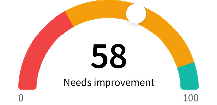
Don't guess if your resume is good enough.
See how it scores against the Physical Design Engineer- Staff to Sr. Staff posting at Qualcomm — free, in seconds.
About the Role
Qualcomm Technologies, Inc. is seeking a highly experienced Clock Physical Design Engineer to develop, optimize, and sign off advanced clocking solutions for next-generation NSP designs. This role involves deep expertise in high-performance clock architecture and implementation, optimizing clock performance, power, variation, noise, and robustness across advanced technology nodes.
Responsibilities
- Own and drive clock physical design methodology, implementation, optimization, and signoff for complex NSP designs.
- Architect, implement, and optimize advanced clock distribution structures, including Clock H-trees, Clock mesh architectures, Clock spine methodologies, Hierarchical clock distribution across block and top-level designs, Clock gating and low-power clock distribution techniques.
- Perform detailed SPICE simulation and transistor-level analysis of critical clock structures.
- Analyze and debug clock-related timing and clock skew, dynamic and leakage power, signal integrity and noise, on-chip variation, jitter and clock uncertainty, duty-cycle distortion, slew and waveform degradation, and physical implementation and routing issues.
- Drive clock convergence and signoff across multiple modes, process corners, voltage conditions, temperatures, and operating frequencies.
- Analyze clock distribution tradeoffs across performance, power, area, skew, insertion delay, variation, and robustness, and recommend appropriate clock architectures and implementation strategies.
- Provide technical feedback and guidance to Physical Design engineers on required clocking fixes, clock tree/mesh/spine optimization opportunities, clock routing and physical implementation issues, timing and variation concerns, power reduction opportunities, and potential signoff risks.
- Collaborate closely with PLL, STA/timing, power, CAD, RTL, architecture, and implementation teams to align clock source assumptions, PLL and clock-source characteristics, jitter budgets, clock uncertainty, clock latency and skew targets, variation assumptions, MMMC constraints, and clock signoff methodology.
- Perform detailed clock timing analysis using Synopsys PrimeTime and correlate implementation, STA, extraction, and SPICE results.
- Work with implementation teams to develop and tune customized clock implementation recipes and methodologies for aggressive performance and power targets.
- Support clock-related ECO development and implementation during timing closure and tapeout convergence.
- Evaluate clock networks for IR-drop, EM, crosstalk, signal integrity, and reliability risks, and work with implementation and power-integrity teams to resolve issues before tapeout.
- Drive clock-related tapeout readiness and ensure all clock structures meet required timing, power, physical verification, and reliability signoff criteria.
- Develop and enhance clock analysis, debug, characterization, and implementation automation using TCL, Python, Perl, and Linux shell scripting.
Requirements
- Bachelor’s or Master’s degree in Electrical Engineering, Computer Engineering, or related field.
- 10+ years of industry experience in ASIC/SoC Physical Design, with significant hands-on experience in high-performance clock implementation and timing closure.
- Proven experience taking complex ASIC/SoC designs through physical design convergence and successful tapeout.
- Deep hands-on expertise with advanced clock distribution methodologies, including Clock H-trees, Clock mesh, Clock spines, Hierarchical clock distribution, and Clock gating and low-power clock implementation.
- Strong understanding of clock skew and insertion delay, jitter and clock uncertainty, slew and duty-cycle distortion, PVT and on-chip variation, clock power optimization, clock signal integrity, clock-related IR/EM concerns, and multi-mode/multi-corner timing analysis.
- Hands-on experience with SPICE simulation and the ability to analyze clock circuits and distribution structures at the transistor and waveform level.
- Strong experience with industry-standard Physical Design and signoff tools, including Synopsys Fusion Compiler / ICC2 and/or Cadence Innovus, Synopsys PrimeTime, RC extraction and signal-integrity analysis tools, and Physical verification and DRC/LVS signoff flows.
- Strong understanding of advanced-node timing, parasitics, variation, power integrity, and reliability effects on clock distribution.
- Proficiency in TCL, Python, Perl, and Linux/Unix environments.
Skills
- Clock H-trees
- Clock mesh architectures
- Clock spine methodologies
- Hierarchical clock distribution
- Clock gating
- Low-power clock distribution
- SPICE simulation
- Transistor-level analysis
- Timing analysis
- Clock skew
- Jitter
- Clock uncertainty
- Duty-cycle distortion
- Slew
- Waveform degradation
- Physical implementation
- Routing
- Synopsys PrimeTime
- TCL scripting
- Python scripting
- Perl scripting
- Linux shell scripting
- Custom clock methodologies
- Advanced technology nodes
- PLL behavior
- Clock-source modeling
- Clock uncertainty budgeting
- IR-drop analysis
- Electromigration analysis
- Signal integrity analysis
- Crosstalk analysis
- Reliability analysis
- SoC implementation
- Debugging
Location
- USA
Work Type
- Full-time
Experience Level
- 10+ years of ASIC/SoC physical design experience
- 6+ years of ASIC design, verification, validation, integration, or related work experience (with Bachelor's)
- 5+ years of ASIC design, verification, validation, integration, or related work experience (with Master's)
- 4+ years of ASIC design, verification, validation, integration, or related work experience (with PhD)
Education Level
- Bachelor's degree in Science, Engineering, or related field
- Master's degree in Science, Engineering, or related field
- PhD in Science, Engineering, or related field
- Bachelor’s or Master’s degree in Electrical Engineering, Computer Engineering, or related field
Salary/Compensations
- $174,400.00 - $261,600.00
Benefits
- Competitive annual discretionary bonus program
- Opportunity for annual RSU grants
- Highly competitive benefits package
About the Company
- Qualcomm Technologies, Inc. is a global leader in wireless technology innovation, powering the connected world and enabling a mobile ecosystem that touches billions of people.
- The NSP Physical Design Team is focused on developing cutting-edge solutions for next-generation network and computing platforms.
Equal Opportunity
- Qualcomm is an equal opportunity employer; all qualified applicants will receive consideration for employment without regard to race, color, religion, sex, sexual orientation, gender identity, national origin, disability, Veteran status, or any other protected classification.
- Qualcomm is committed to providing an accessible process for individuals with disabilities and making our workplace accessible.