Impress employers and recruiters.
Choose from hundreds of resume examples.
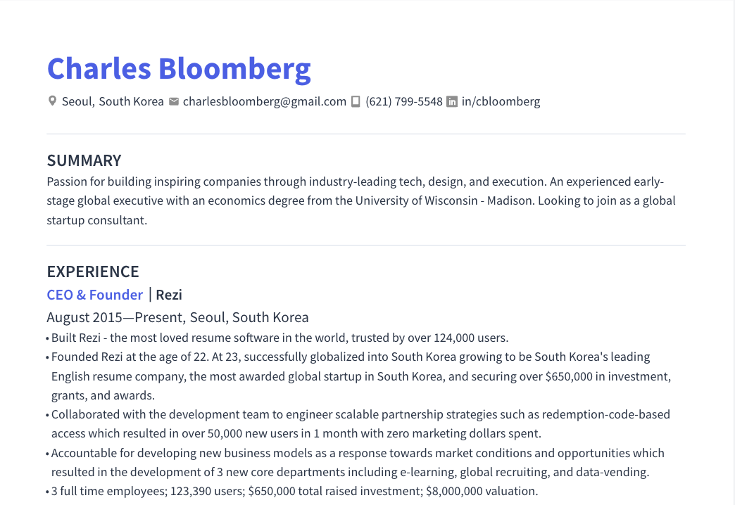
Impress employers and recruiters.
Choose from hundreds of resume examples.
Tailor your resume to this Advanced Packaging Engineer role.
Rezi rewrites your resume against Volantis Semiconductor, Inc.'s job description. Free.
Tailor your resume to this Advanced Packaging Engineer role.
Rezi rewrites your resume against Volantis Semiconductor, Inc.'s job description. Free.
Don't guess if your resume is good enough.
See how it scores against the Advanced Packaging Engineer posting at Volantis Semiconductor, Inc. — free, in seconds.
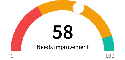
Don't guess if your resume is good enough.
See how it scores against the Advanced Packaging Engineer posting at Volantis Semiconductor, Inc. — free, in seconds.
About the Role
Contribute to and own aspects of the Volantis A-0 and A-1 package, focusing on package design or process development for wafer-scale packages with silicon and compound semiconductor dies. Address challenges in warpage, CTE mismatch, thermomechanical aspects, and assembly speed to enable a new era of AI by breaking the memory wall.
Responsibilities
- Contribute to and own aspects of the Volantis A-0 and A-1 package.
- Design or process development of complex packages.
- Work with architects to co-design system architecture and package design.
Requirements
- Ability to think from first principles about novel problems.
- Understanding that solutions for 5x reticle platforms may not work for 56x reticle platforms.
Skills
- Package design
- Package process development
- Heterogeneous material assemblies
- High-TDP packages
- Compound semiconductor assemblies
- Co-packaged optics
- Interposer platforms (CoWoS, CoWoS-L, CoWoS-R, EMIB, FoCoS, FoCoS-Bridge, etc.)
- Flip-chip integration (mass reflow, TCB & LAB)
- Large scale substrates (>50x50mm)
Salary/Compensations
- $250K-$400K
Benefits
- Competitive Base salary
- Significant Equity Stake
About the Company
- Building a wafer-scale package with both silicon and compound semiconductor dies sitting together at very high TDP.
- The end result is breaking the memory wall, enabling a new era of AI, and a platform that scales another 1-3 orders of magnitude.