Impress employers and recruiters.
Choose from hundreds of resume examples.
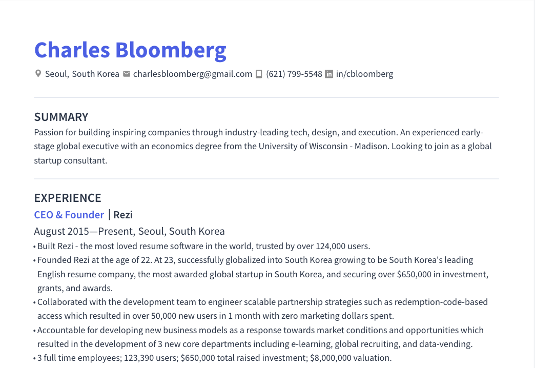
Impress employers and recruiters.
Choose from hundreds of resume examples.
Tailor your resume to this Micro-Optics Engineer role.
Rezi rewrites your resume against Volantis Semiconductor, Inc.'s job description. Free.
Tailor your resume to this Micro-Optics Engineer role.
Rezi rewrites your resume against Volantis Semiconductor, Inc.'s job description. Free.
Don't guess if your resume is good enough.
See how it scores against the Micro-Optics Engineer posting at Volantis Semiconductor, Inc. — free, in seconds.
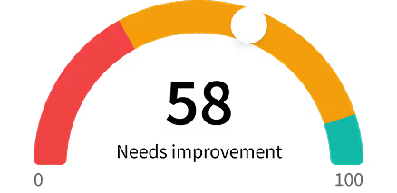
Don't guess if your resume is good enough.
See how it scores against the Micro-Optics Engineer posting at Volantis Semiconductor, Inc. — free, in seconds.
About the Role
We are seeking a Senior Micro-Optics/Microlens Array Engineer to design, model, and validate microlens-array and wafer-level micro-optical components for high-density photonic packages. You will translate system-level optical requirements into manufacturable designs, build tolerance budgets, work with fabrication and packaging partners, and close the loop with measured data.
Responsibilities
- Own micro-optical design, including lens pitch, aperture, focal length, numerical aperture, sag, surface form, fill factor, array uniformity, substrate, material, and coating choices.
- Build connected optical models using tools such as Zemax OpticStudio, Code V, FRED, LightTools, VirtualLab, Ansys/Lumerical, COMSOL, or equivalent.
- Bridge EM-scale and package-scale design by connecting electromagnetic simulations to system-level optical models.
- Develop sensitivity studies and tolerance budgets across fabrication, placement, package stack-up, and environmental variations.
- Partner with process and supplier teams across lithography, patterning, etch transfer, deposition, thin-film coatings, and metrology.
- Create vendor-ready specifications, optical prescriptions, mechanical drawings, material and coating requirements, and metrology plans.
- Evaluate fabrication routes such as photoresist reflow, grayscale lithography, etch transfer, molding, and replication.
- Plan and run prototype characterization, including surface profile, focal length, and optical throughput.
- Build Python tools for simulation sweeps, tolerance studies, data reduction, visualization, and reporting.
- Partner with packaging, mechanical, thermal, test, reliability, device, and system teams to move designs from concept to qualified hardware.
Requirements
- M.S. or Ph.D. in Optical Engineering, Electrical Engineering, Applied Physics, Physics, Photonics, Mechanical Engineering, Materials Science, or a related field; B.S. with exceptional relevant experience also considered.
- Industry experience in micro-optics, wafer-level optics, optical design, photonic packaging, optomechanics, precision optics, semiconductor process integration, or advanced optoelectronic hardware.
- Experience designing microlens arrays, aspheric micro-optics, diffractive or hybrid micro-optical surfaces, compact optical elements, or package-level optical features with manufacturing constraints.
- Proficiency with optical modeling and tolerancing in Zemax OpticStudio, Code V, FRED, LightTools, VirtualLab, Ansys/Lumerical, COMSOL, or equivalent.
- Ability to convert requirements into an optical design, tolerance budget, supplier data package, and practical characterization plan.
- Experience with prototype characterization, failure analysis, design iteration, and model-to-hardware correlation.
- Python skills for simulation automation, numerical analysis, data reduction, and reporting.
- Clear written and verbal communication.
- Ability to operate independently in a fast-changing startup environment.
Skills
- Micro-optics
- Microlens array design
- Optical design
- Optical modeling
- Zemax OpticStudio
- Code V
- FRED
- LightTools
- VirtualLab
- Ansys/Lumerical
- COMSOL
- FDTD
- FEM
- EME
- RCWA
- Tolerancing
- Yield analysis
- Monte Carlo methods
- DOE methods
- Semiconductor process awareness
- Lithography
- Grayscale patterning
- Imprint
- Etch transfer
- Deposition
- Thin-film coatings
- Wafer-level metrology
- Design rules
- Process-window trade-offs
- Vendor specifications
- Optical prescriptions
- Mechanical drawings
- Metrology plans
- Incoming inspection criteria
- Acceptance criteria
- Fabrication routes
- Photoresist reflow
- Molding
- Replication
- Prototype characterization
- Surface profile
- Focal length
- Array uniformity
- Optical throughput
- Reflection behavior
- Polarization sensitivity
- Thermal drift
- Environmental stability
- Alignment sensitivity
- Python
- Simulation automation
- Data reduction
- Visualization
- Dashboards
- Technical reporting
- Cross-functional collaboration
- Packaging
- Mechanical engineering
- Thermal engineering
- Test engineering
- Reliability engineering
- Device engineering
- System engineering
- Wafer-level optics
- Optomechanics
- Precision optics
- Semiconductor process integration
- Advanced optoelectronic hardware
- Aspheric micro-optics
- Diffractive surfaces
- Hybrid micro-optical surfaces
- Compact optical elements
- Package-level optical features
- Manufacturing constraints
- EM-to-system optical modeling
- Microfabrication
- Process variation
- DFM
- Failure analysis
- Model-to-hardware correlation
- Numerical analysis
- Written communication
- Verbal communication
- Independent operation
- Startup environment
- Concept development
- Prototype builds
- Supplier qualification
- Production ramp
- High-density optoelectronic packages
- Semiconductor photonics packages
- Optical interconnect hardware
- Co-packaged optics
- Sensing systems
- LiDAR
- AR/VR optics
- Miniature imaging
- Datacom hardware
- Mask review
- Layout review
- Critical-dimension data
- SEM interpretation
- AFM interpretation
- Profilometry interpretation
- Film-stack review
- Process-control limits
- Foundry interaction
- Process team interaction
- DVT
- Reliability screening
- Thermal cycling
- Humidity exposure
- High-temperature storage
- Environmental qualification
- Optomechanical CAD
- GD&T
- SolidWorks
- NX
- Creo
- Zemax CAD exchange
- Lab automation
- Motion stages
- Cameras
- Optical power meters
- OSAs
- Temperature controllers
- SMUs
- Oscilloscopes
- PyVISA
- SCPI
- LabVIEW
- Owner mindset
- Bias for action
- Cross-functional fluency
- Builder mentality
Experience Level
- Senior
Education Level
- M.S. or Ph.D. in Optical Engineering, Electrical Engineering, Applied Physics, Physics, Photonics, Mechanical Engineering, Materials Science, or a related field; B.S. with exceptional relevant experience also considered.
About the Company
- We do not expect one person to match every item below. Strong candidates from micro-optics, optical packaging, semiconductor photonics, lithography/process integration, precision optics, or FDTD-Zemax co-design backgrounds are encouraged.
- This section is a guide, not a rigid checklist. We care most about evidence of technical ownership, sound physics, manufacturability judgment, and the ability to learn quickly.
- Owner mindset: drive ambiguous technical problems from first principles to measured hardware.
- Bias for action: build lightweight experiments, define clear metrics, and iterate based on data.
- Cross-functional fluency: communicate trade-offs across optics, semiconductor process, packaging, mechanical, thermal, test, reliability, and systems teams.
- Builder mentality: create reusable models, scripts, specifications, and test methods.