Impress employers and recruiters.
Choose from hundreds of resume examples.
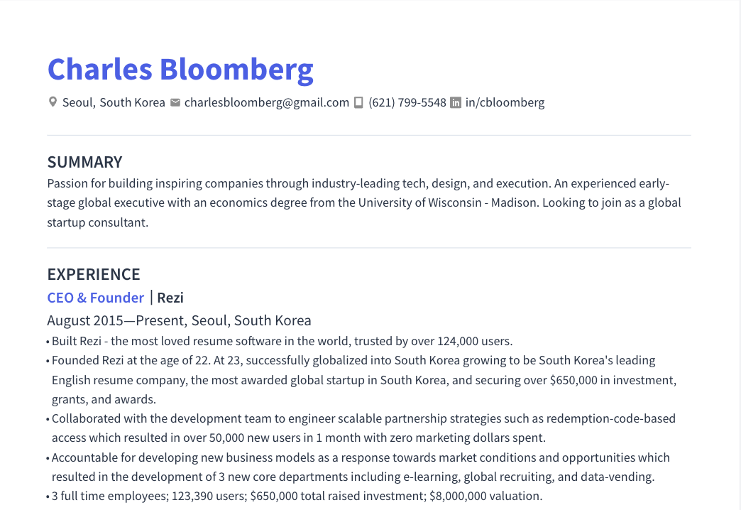
Impress employers and recruiters.
Choose from hundreds of resume examples.
Tailor your resume to this Packaging Engineer- Bump Interconnect role.
Rezi rewrites your resume against Volantis Semiconductor, Inc.'s job description. Free.
Tailor your resume to this Packaging Engineer- Bump Interconnect role.
Rezi rewrites your resume against Volantis Semiconductor, Inc.'s job description. Free.
Don't guess if your resume is good enough.
See how it scores against the Packaging Engineer- Bump Interconnect posting at Volantis Semiconductor, Inc. — free, in seconds.
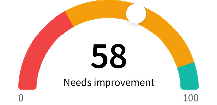
Don't guess if your resume is good enough.
See how it scores against the Packaging Engineer- Bump Interconnect posting at Volantis Semiconductor, Inc. — free, in seconds.
About the Role
Lead bump interconnect development for advanced semiconductor devices (2.5D/3D/chiplet/fan-out), covering metallurgy, RDL design, plating, pad design, OSAT engagement, reliability, failure analysis, and cross-functional support through productization.
Responsibilities
- Own end-to-end bump interconnect development for ubump and C4 processes, including bump formation and reflow for various chip attach methods.
- Define and own bump metallurgy stacks for ubump and C4 interconnects, including UBM selection and pad finish specifications.
- Develop and own design rules for bump interconnects, covering pitch, diameter, standoff height, keep-outs, and land pad geometry.
- Lead RDL process development, including electroplating, via fills, pad finishes, and RDL design rules.
- Collaborate with OSATs and bumping foundries to qualify processes, align design rules, and manage production transfers.
- Evaluate and mitigate assembly risks such as non-wet opens, voiding, head-in-pillow, intermetallic growth, and joint fatigue.
- Perform root cause analysis of failures using cross-sectioning, SEM, CSAM, and other failure analysis techniques.
- Support reliability qualification through thermal cycling, drop, mechanical shock, and power cycling.
- Work cross-functionally with design, reliability, thermal, and manufacturing teams to ensure robust package performance.
Requirements
- Industry experience in semiconductor packaging with strong emphasis on bump interconnect processes, RDL development, and productization.
Skills
- ubump (micro-bump) and C4 bumping processes
- Bumping metallurgy (UBM stacks, solder alloy systems, intermetallic compound formation)
- RDL plating processes (Cu electroplating, photoresist patterning, seed layer deposition)
- Thermo-mechanical behavior in bump interconnect assemblies
- Failure analysis and reliability testing (cross-sections, SEM, CSAM, thermal cycling)
- OSAT and supplier collaboration for process development and transfer
- Problem-solving and debugging yield and reliability issues
- III-V packaging
- Photonics packaging
- Precision chip attach
- Advanced packaging technologies (2.5D interposers, 3D stacking, chiplets, CoWoS-like architectures)
- Fine-pitch micro-bump and hybrid bonding approaches
- Integrating high-power or high-TDP devices
- Thermo-mechanical modeling
- System-level interactions (warpage, second-level interconnect reliability)
- Bump metallurgy fundamentals (UBM stack design, solder alloy selection, wetting behavior)
- Intermetallic compound (IMC) formation, growth kinetics, and phase behavior in Cu/Sn, Ni/Sn, and Au/Sn systems
Experience Level
- Experienced engineer