Impress employers and recruiters.
Choose from hundreds of resume examples.
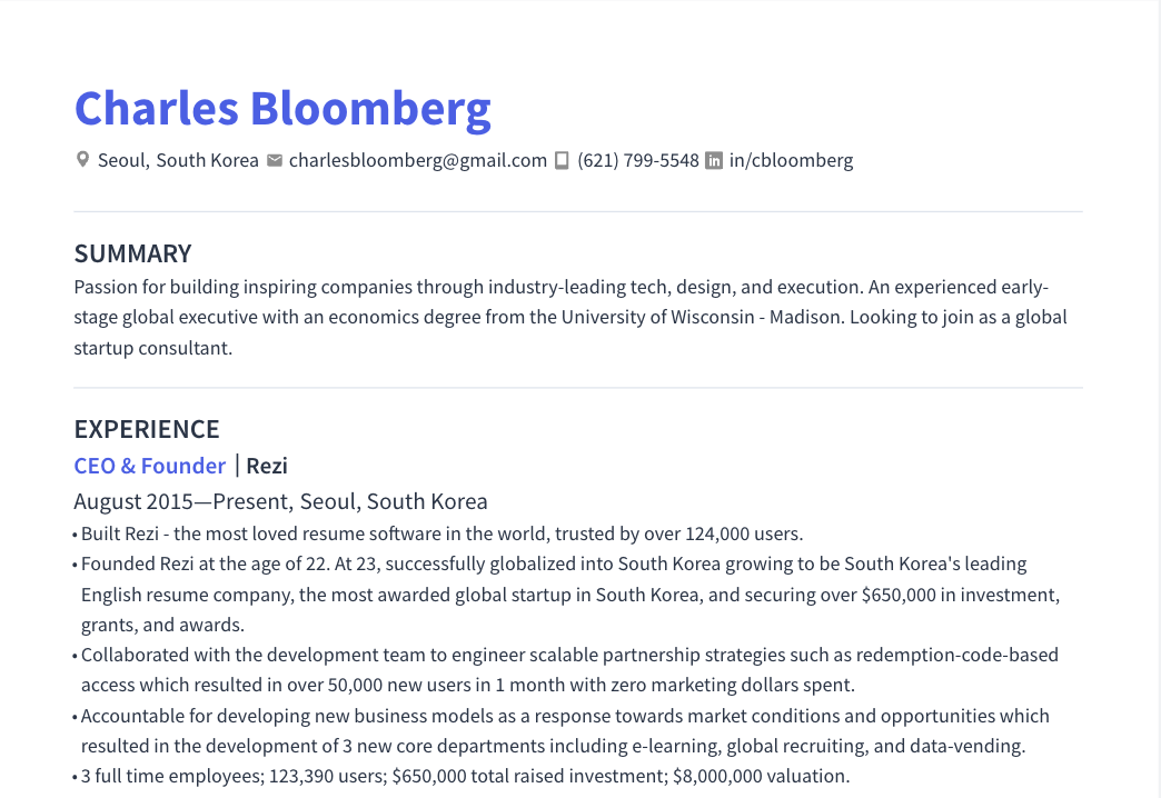
Impress employers and recruiters.
Choose from hundreds of resume examples.
Tailor your resume to this Packaging Engineer- Materials role.
Rezi rewrites your resume against Volantis Semiconductor, Inc.'s job description. Free.
Tailor your resume to this Packaging Engineer- Materials role.
Rezi rewrites your resume against Volantis Semiconductor, Inc.'s job description. Free.
Don't guess if your resume is good enough.
See how it scores against the Packaging Engineer- Materials posting at Volantis Semiconductor, Inc. — free, in seconds.
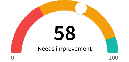
Don't guess if your resume is good enough.
See how it scores against the Packaging Engineer- Materials posting at Volantis Semiconductor, Inc. — free, in seconds.
About the Role
Seeking an experienced engineer to lead wafer level mold and underfill process development for advanced semiconductor packages. This role involves material selection, qualification, process development, and cross-functional support through productization.
Responsibilities
- Develop and optimize wafer level molding processes including compression molding, transfer molding, and mold underfill (MUF) for fan-out and advanced heterogeneous packages.
- Own mold compound and underfill material selection and qualification, including evaluation of filler content, CTE, modulus, Tg, viscosity, and moisture uptake to meet thermo-mechanical and reliability requirements.
- Drive underfill process development including capillary underfill (CUF) dispense strategies, flow and void optimization, and cure profile development for high-density flip chip and chiplet assemblies.
- Evaluate and mitigate assembly risks including warpage, delamination, void formation, bleed-out, mold flash, and filler settling; define process windows and controls to ensure repeatable yield across wafer and panel formats.
- Collaborate with OSATs and material suppliers to qualify mold and underfill materials, define dispense and cure equipment requirements, and manage process transfers into production.
- Lead characterization of mold and underfill material properties (viscosity, gel time, cure kinetics, adhesion, CTE, modulus) and correlate material behavior to process outcomes and package reliability.
- Work closely with thermal mechanical modeling teams to model solder joint reliability of bump interconnects with various underfills and predict warpage with various mold compounds.
- Support reliability qualification including thermal cycling, drop, mechanical shock, and power cycling.
- Work cross-functionally with design, reliability, thermal, and manufacturing teams to ensure robust package performance from concept through high-volume production.
Requirements
- Strong experience in wafer level molding and underfill processes for advanced semiconductor packages including fan-out wafer level packaging (FOWLP), 2.5D, and chiplet architectures.
- Deep understanding of mold compound and underfill material science including epoxy resin systems, filler particle size and loading, cure chemistry, and how material properties drive thermo-mechanical package behavior.
- Experience with underfill dispense techniques (capillary, no-flow, mold underfill), flow and void characterization, bleed-out control, and cure process optimization including staged and snap cure profiles.
- Understanding of thermo-mechanical behavior driven by mold and underfill materials including CTE mismatch, warpage evolution through cure and reflow, delamination driving forces, and material-induced reliability risks.
- Hands-on experience with failure analysis of mold and underfill failures including cross-sections, SEM/EDS, CSAM, TGA, DSC, and DMA for material characterization and thermal cycling reliability evaluation.
- Ability to work with OSATs and material suppliers to develop, qualify, and transfer mold and underfill processes into production, including equipment setup and process control plans.
- Strong problem-solving skills with ability to debug mold and underfill yield and reliability issues in manufacturing environments, including DOE-driven process optimization.
Skills
- Wafer level molding
- Underfill processes
- Fan-out wafer level packaging (FOWLP)
- 2.5D packaging
- Chiplet architectures
- Mold compound material science
- Underfill material science
- Epoxy resin systems
- Filler particle size and loading
- Cure chemistry
- Thermo-mechanical behavior
- CTE mismatch
- Warpage analysis
- Delamination analysis
- Reliability analysis
- Failure analysis
- Cross-sections
- SEM/EDS
- CSAM
- TGA
- DSC
- DMA
- Process development
- Material qualification
- Assembly integration
- OSAT collaboration
- Supplier management
- Process transfer
- Equipment requirements definition
- Process control plans
- DOE
- Underfill materials for III-V or photonics packaging
- Optically clear encapsulants
- Low-modulus underfills
- 2.5D interposers
- 3D stacking
- CoWoS-like structures
- High-power device packaging
- High-TDP device packaging
- High thermal conductivity materials
- Thermo-mechanical modeling
- Simulation collaboration
- System-level interactions
- TIM application
- Cold plate interaction
Experience Level
- Experienced engineer